FinFET Technology Market Forecasted to Surpass USD 349.50 Billion with 21.7% CAGR by 2035
FinFET Technology Market Size, Share and Research Report By Technology Node (22 nm, 16/14 nm, 10 nm, 7 nm, 5 nm and
Press Release Disclaimer: This is a press release distributed through the XPR Media network. It has not been independently verified by our newsroom.

FinFET Technology Market Size, Share and Research Report By Technology Node (22 nm, 16/14 nm, 10 nm, 7 nm, 5 nm and Below), By Foundry Business Model
NEW YORK,, NY, UNITED STATES, September 18, 2026 /EINPresswire.com/ — ➤ Market Overview
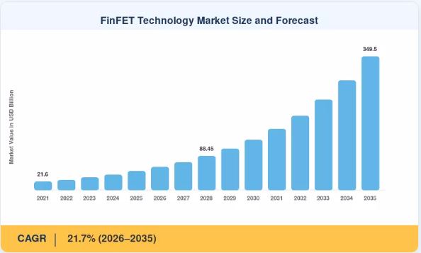
The FinFET Technology Market closed 2025 at USD 49.07 billion and enters the forecast window at USD 59.72 billion in 2026, climbing to USD 349.50 billion by 2035 at a 21.7% CAGR. This expansion reflects the semiconductor industry’s continued shift toward three-dimensional transistor architecture as manufacturers push past the electrostatic limits of planar CMOS at advanced process nodes.
Asia-Pacific commanded 57.0% of the FinFET Technology Market in 2025, supported by concentrated foundry capacity, large-scale mobile chipset production, and an expanding base of design and fabrication investment across the region. Chipmakers are increasingly directing capital toward fin-based process nodes as smartphone, computing, and AI accelerator demand continues to climb.
Asia-Pacific is also advancing at a 22.1% CAGR across the forecast period, making it the fastest-growing region for FinFET technology even while holding the largest existing share. Greenfield fabrication investment in Japan, India, and Singapore, combined with sustained foundry expansion in Taiwan and South Korea, is creating substantial opportunities across the semiconductor value chain.
The Middle East & Africa is emerging as the fastest-growing region outside Asia at roughly a 23.4% CAGR, supported by sovereign artificial intelligence compute programs and national semiconductor strategies. Governments and enterprises are focusing on secure compute access, localized data infrastructure, and long-term technology partnerships, creating additional downstream demand for FinFET-based accelerator and processor silicon.
Download Sample Pages of Research Overview –
https://www.marketresearchfuture.com/sample_request/6724
➤ FinFET Technology Industry Landscape
FinFET, or Fin Field-Effect Transistor, technology replaces the flat gate structure of planar transistors with a raised, fin-shaped channel that the gate wraps around on three sides. This design gives chipmakers substantially better control over current leakage and switching behavior, allowing continued transistor scaling well past the point where planar architectures lose reliable electrostatic control.
The growing complexity of leading-edge semiconductor manufacturing is strengthening demand for fin-based process technology. Foundries are increasingly retiring older planar lines for cost-sensitive production while directing new capital toward 7 nm, 5 nm, and emerging 3 nm fin-based nodes. Design houses, equipment suppliers, and materials providers coordinate closely across this ecosystem to keep pace with tightening performance, power, and area requirements.
The Advanced Packaging Market is a relevant topical authority keyword because packaging technology increasingly determines how much value chipmakers can extract from FinFET-based silicon. Techniques such as chiplet integration, hybrid bonding, and silicon interposers allow multiple fin-based dies to be combined into a single system, extending performance gains after traditional lithographic scaling slows.
The connection between advanced packaging and FinFET technology demonstrates how semiconductor value is shifting from the front-end wafer process to back-end integration. As chipmakers deploy AI accelerators and heterogeneous compute systems, they require packaging capacity that can keep pace with die complexity, thermal density, and interconnect bandwidth. These requirements create opportuneities for packaging specialists across the broader semiconductor equipment and materials ecosystem.
➤ Key Growth Drivers
The rapid buildout of artificial intelligence infrastructure remains a major growth driver for the FinFET Technology Market. Hyperscale data center operators are deploying large volumes of accelerator and processor silicon fabricated on fin-based nodes to support training and inference workloads. However, this demand also introduces capacity constraints, encouraging foundries to prioritize allocation for high-value accelerator programs.
Government-backed fabrication investment is another significant factor supporting industry expansion. Programs such as the United States CHIPS and Science Act and the European Chips Act are channeling substantial public and private capital toward domestic fabrication capacity. Because subsidy conditions generally favor leading-edge logic, this funding is directed almost entirely toward fin-based and successor transistor architectures.
➤ AI Accelerator and Data Center Demand
AI accelerator demand is creating substantial opportunities because hyperscale operators require reticle-limit die fabricated on the most advanced available fin-based nodes. Different workloads carry different requirements related to power envelope, memory bandwidth, and thermal budget. Foundries are prioritizing capacity for these programs given their scale and long qualification cycles.
Mobile and consumer electronics demand is also becoming more common as smartphone shipments recover and on-device intelligence features expand. However, growing die complexity can create challenges involving cost, yield, and thermal management. Fin-based process technology helps address these operations through improved leakage control, higher transistor density, and better performance-per-watt characteristics.
➤ Artificial Intelligence and Automation in Chip Design
Artificial intelligence and automation are transforming semiconductor design by enabling engineering teams to identify layout inefficiencies, forecast yield outcomes, automate routine verification tasks, and optimize transistor placement. AI-assisted design tools can analyze large quantities of process information and identify potential issues before they significantly affect production schedules.
Automation can also reduce manual intervention across mask design, defect classification, and process control. As chipmakers increasingly pursue fin-based and successor architectures, the demand for design tools capable of supporting intensive and variable workloads is expected to rise. This creates an important intersection between FinFET technology, electronic design automation, analytics, and intelligent process control.
Buy Now Get Comprehensive Market Insights –
https://www.marketresearchfuture.com/checkout?currency=one_user-USD&report_id=6724
➤ Sovereign Fabrication and Supply Chain Security
Supply chain security and regulatory compliance are increasingly central to national semiconductor strategies. Countries operating in defense, communications, and critical infrastructure sectors must secure dependable access to leading-edge logic while complying with export control and technology transfer requirements. Foundries and design houses can support these needs through geographically diversified capacity, qualified second sources, and transparent supply chain reporting.
Data and compute sovereignty is becoming particularly important as governments introduce requirements concerning where AI workloads are processed and where accelerator silicon is sourced. Sovereign compute investments, including those contributing to the Middle East & Africa’s growth, demonstrate the increasing importance of secure, localized infrastructure. Suppliers that understand regional regulations and export requirements can therefore gain competitive advantages.
➤ Technology Node Segmentation
The FinFET Technology Market can be segmented across technology nodes including 22 nm, 16/14 nm, 10 nm, 7 nm, and 5 nm and below. The 7 nm node remains important because it balances proven manufacturing maturity against acceptable power characteristics, keeping fab utilization high across handset, accelerator, and automotive production.
The 5 nm and below segment represents another high-growth area because cloud training workloads increasingly require lower power envelopes at higher transistor density. Legacy nodes such as 22 nm and 16/14 nm continue to serve cost-sensitive automotive, networking, and industrial applications, helping chipmakers balance capacity across a wide range of end markets while reducing the complexity of maintaining every process generation at scale.
➤ Foundry and Design Adoption Trends
Large pure-play foundries remain important participants because they operate complex, capital-intensive fabrication environments and often manage substantial multi-customer wafer volumes. These organizations require advanced process control, yield management, and packaging integration capabilities to serve a broad base of fabless design customers.
Integrated device manufacturers are also becoming an increasingly important customer and supplier segment. Vertically integrated players may reopen external foundry lines to fill capacity, giving fabless and systems companies access to specialized fin-based process technology through service-based models without requiring their own fabrication investment.
➤ Regional Insights
Asia-Pacific held 57.0% of the FinFET Technology Market in 2025, reflecting its established foundry ecosystem and high level of leading-edge fabrication capacity. The region benefits from the presence of major foundries, equipment suppliers, and large fabless design companies pursuing advanced process technology. Demand for mobile SoC, AI accelerator, and consumer electronics production remains strong.
North America held 24.2% of the market in 2025 and continues to grow as subsidy-backed fabrication projects advance in Arizona, Ohio, and Texas. Growing internet penetration, expanding accelerator demand, and technology investments are expected to support fin-based semiconductor production across both established and emerging fabrication hubs.
The Middle East & Africa is developing as an important opportunity because sovereign compute programs and national digitization initiatives are increasing demand for accelerator silicon. The region is expanding at roughly a 23.4% CAGR, with investments in localized data infrastructure, artificial intelligence platforms, and government digitization supporting future expansion.
Emerging Opportunities
One of the most significant opportunities involves fin-based silicon for AI and data-intensive workloads. Chipmakers increasingly need specialized process technology to support artificial intelligence, machine learning, analytics, and large-scale data processing. Foundries capable of optimizing these workloads while controlling cost per transistor can create differentiated offerings within the broader semiconductor ecosystem.
Another opportunity is the development of automotive-qualified fin-based derivative nodes. Healthcare, automotive, industrial, and telecommunications organizations have different compliance, reliability, and performance requirements. Foundries that combine leading-edge process technology with sector-specific qualification can offer more targeted solutions and build stronger long-term customer relationships.
➤ Key Challenges
Despite strong growth potential, the industry faces several challenges. Leading-edge fabrication can become extremely expensive as wafer and tooling costs rise, making capital efficiency a critical requirement. Chipmakers may also encounter yield variability, integration difficulties, export control complexity, and shortages of skilled process engineering talent.
Supply chain security and compliance remain ongoing concerns. Foundries must maintain strong governance and process control practices while ensuring that customer designs are protected across increasingly distributed manufacturing and packaging operations. Capacity interruptions can also have significant consequences, making reliability, redundancy, and qualified second sourcing essential components of successful fin-based supply strategies.
➤ Future Outlook
The FinFET Technology Market is expected to maintain steady expansion as chipmakers increasingly rely on fin-based architecture for mission-critical accelerator, mobile, and automotive applications. Growth from USD 49.07 billion in 2025 to USD 349.50 billion by 2035 represents a substantial increase in demand for advanced process technology, packaging integration, automation, and sovereign fabrication capacity.
Future development will increasingly center on architectural coexistence with next-generation gate-all-around nanosheet devices, expanded advanced packaging capacity, energy-efficiency-driven node selection, and geographically diversified fabrication. Suppliers that can combine technical expertise with strong process control, cost optimization, and flexible capacity models will be well positioned to capture long-term opportunities.
Browse Full Report Details – https://www.marketresearchfuture.com/reports/finfet-technology-market-6724
➤ Key Takeaways
The FinFET Technology Market is being shaped by AI accelerator demand, government-backed fabrication investment, advanced packaging integration, automotive electrification, and continued mobile chipset growth. Asia-Pacific remains the leading regional contributor, while North America benefits from subsidy-backed fab construction and the Middle East & Africa demonstrates strong growth potential through sovereign compute investment.
The integration of AI, automation, and advanced packaging will increasingly redefine how value is captured across fin-based semiconductor production. At the same time, related technology areas such as the Advanced Packaging Market demonstrate the growing requirement for scalable, secure, and high-performance compute infrastructure. As chipmakers prioritize resilience and process efficiency, FinFET technology is expected to remain a strategic component of the global semiconductor industry through the next decade.
➤ Frequently Asked Questions
What does a leading-edge tape-out actually cost a design team?
A full 7 nm flow including masks, IP licensing, and verification runs roughly USD 105–160 million; 5 nm pushes past USD 230 million. Multi-project wafer shuttles cut prototype spend by about 70% for low-volume programs
How do fin-based and gate-all-around nanosheet devices compare for buyers?
Nanosheet delivers higher drive current per footprint and finer threshold tuning. Fin-based libraries, however, carry a decade of silicon-proven IP, so most 2026–2028 derivative products stay with them for schedule certainty.
➤➤➤ Industry Analysis Reports by Market Research Future:
Embedded Technology Market-
https://www.marketresearchfuture.com/reports/embedded-technology-market-1041
Capacitive Sensor Market-
https://www.marketresearchfuture.com/reports/capacitive-sensor-market-1077
Access Control Market-
https://www.marketresearchfuture.com/reports/access-control-market-1089
Digital Signage Market-
https://www.marketresearchfuture.com/reports/digital-signage-market-1102
Intelligent Virtual Assistant Market-
https://www.marketresearchfuture.com/reports/intelligent-virtual-assistant-market-1147
Smartphone Display Market-
https://www.marketresearchfuture.com/reports/smartphone-display-market-1172
Flexible Printed Circuit Board Market-
https://www.marketresearchfuture.com/reports/flexible-printed-circuit-board-market-1198
Mechanical Keyboard Market-
https://www.marketresearchfuture.com/reports/mechanical-keyboard-market-1215
Facial Recognition Market-
https://www.marketresearchfuture.com/reports/facial-recognition-market-1250
Gesture Recognition And Touchless Sensing Market-
https://www.marketresearchfuture.com/reports/gesture-recognition-touchless-sensing-market-1270
Market Research Future
Market Research Future
+ +1 855-661-4441
email us here
Legal Disclaimer:
EIN Presswire provides this news content “as is” without warranty of any kind. We do not accept any responsibility or liability
for the accuracy, content, images, videos, licenses, completeness, legality, or reliability of the information contained in this
article. If you have any complaints or copyright issues related to this article, kindly contact the author above.

Media gallery